 Placement of the AC inverter
 Up
Up
Here you will find several schematics. I will update them as my design evolves, and will soon post a Excel compatible spreadsheet with my calculations.
The logical organization of my drive is as follows:
I use a 15V regulated switching mode power supply.
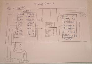
I use a signal generator chip XR2206 (see datasheet).The future control module is a module that will enable me in the future to add control functions switching DCEN, DCEP and squarewave without using a heavy and cumberson commutator switch. For now, signal output of XR2206 simply goes to the inputs of comparator.
Since gate drives require separate high and low end signals, I use a LM339 quad comparator see datasheet) to generate the signals that always are logical opposites of one another. One is the input to the high side, another to low side, ensuring that they are never TRUE at the same time.
I will use four Toshiba MG200Q2YS40 (see this PDF) IGBTs, each representing a full half bridge with freewheeling diodes. That means that I will have two parallel H bridges.
 |
| Schematic of the timing circuit. |
